Introduction:
The Metal-Oxide-Semiconductor Field-Effect Transistor MOSFET is a crucial component of modern electronic devices, enabling the amplification and switching of electrical signals. In this blog post, we will delve into the intricate details of MOSFETs, exploring their structure and the key factors scientists consider during their design and fabrication.
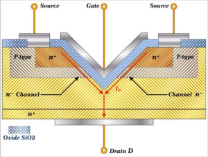
MOSFET Structure:
A MOSFET consists of four main components:
- Substrate: Usually made of silicon, it provides the foundation for the MOSFET’s structure.
- Gate: Located between the source and drain regions, it controls the flow of current within the channel.
- Source: The region where the majority carriers (electrons for N-channel MOSFETs, holes for P-channel MOSFETs) enter the channel.
- Drain: The region where the majority carriers exit the channel.
MOSFET Operation:
When a voltage is applied to the gate terminal, an electric field is generated across the gate dielectric, modulating the conductivity of the channel.The MOSFET operates in three different regions:
- Cut-Off Region: When the gate voltage is below the threshold voltage (Vth), the MOSFET is in a non-conductive state, and no current flows between the source and drain.
- Triode/Linear Region: When the gate voltage is above Vth, but not sufficiently high, the MOSFET operates in the linear region. The current flowing through the channel is proportional to the gate-source voltage.
- Saturation Region: When the gate voltage is sufficiently high, the MOSFET operates in the saturation region. Because the channel is fully open, and the current is primarily determined by the drain-source voltage.
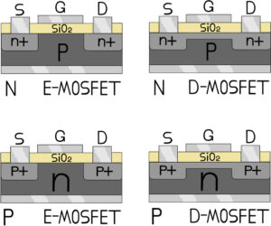
Types of MOSFETs:
There are two main classes of MOSFETs:
- Enhancement Mode MOSFETs: Enhancement mode MOSFETs require a positive voltage at the gate to create a conductive channel between the source and drain. They are normally off when the gate-source voltage is zero. When the gate voltage exceeds the threshold voltage, the channel opens, allowing current to flow. Enhancement mode MOSFETs are widely used in digital logic circuits and switching applications.
- Depletion Mode MOSFETs: Depletion mode MOSFETs, on the other hand, are naturally conducting without an applied voltage at the gate. They are normally on when the gate-source voltage is zero. By applying a negative voltage to the gate, the channel is depleted, reducing the conductance and controlling the current flow. Depletion mode MOSFETs find applications in analog circuits, voltage regulation, and current control.
Each of this class has N-channel and P-chanel:
- N-Channel MOSFET: The majority carriers are electrons, and the channel is created by applying a positive voltage to the gate.
- P-Channel MOSFET: The majority carriers are holes, and the channel is created by applying a negative voltage to the gate.
MOSFET Design Considerations:
Scientists and engineers pay careful attention to various factors during the design and fabrication of MOSFETs:
- Channel Length (L): The length of the channel between the source and drain regions affects the MOSFET’s performance and switching speed. Shorter channel lengths lead to faster operation but may introduce unwanted effects.
- Channel Width (W): The width of the channel determines the current-carrying capacity of the MOSFET. Wider channels can handle higher currents but may increase parasitic capacitances.
- Gate Dielectric: The gate oxide layer separates the gate electrode from the channel. It is typically made of silicon dioxide (SiO2) or high-k dielectric materials to ensure efficient control of the channel.
- Threshold Voltage (Vth): The gate voltage at which the MOSFET starts to conduct current. It can be adjusted by doping the channel region during fabrication.
- Source/Drain Contacts: The source and drain regions are doped to create low-resistance contacts, ensuring efficient current flow.
- Gate Material: The gate electrode is typically made of polycrystalline silicon (polysilicon) or metal materials such as aluminum or copper.
- Passivation Layer: A protective layer is added to prevent contamination, oxidation, or physical damage to the MOSFET.
MOSFET Fabrication:
The fabrication process involves several steps, including:
- Wafer Preparation: The silicon wafer is cleaned and prepared for the subsequent manufacturing steps.
- Thermal Oxidation: A controlled oxidation process forms a thin layer of silicon dioxide on the wafer’s surface, creating the gate dielectric.
- Photo-lithography: A series of photo-resist coatings, exposure to UV light, and chemical etching define the regions where transistors will be formed.
- Ion Implantation: Scientists dope the source and drain regions to create low-resistance contacts, ensuring efficient current flow.
- Metallisation: Manufacturers typically use poly-crystalline silicon (poly-silicon) or metal materials such as aluminium or copper to make the gate electrode.
- Passivation and Packaging: Engineers add a passivation layer to prevent contamination, oxidation, or physical damage to the MOSFET.
- Testing and Quality Control: The fabricated MOSFETs undergo rigorous testing to ensure their functionality and performance meet the desired specifications. This includes electrical testing, leakage current measurements, and reliability assessments.
Advancements and Future Trends:
MOSFET technology has continually advanced, driven by the need for smaller, faster, and more power-efficient devices. Some notable advancements include:
- Scaling: Shrinking the dimensions of MOSFETs to nano-scale sizes, such as FinFETs and nano-wire MOSFETs, to enhance performance and packing density.
- High-k Dielectrics: Introducing high-k dielectric materials to replace traditional silicon dioxide gate oxides, thus enabling better control over the channel and reducing leakage currents.
- Strained Silicon: Applying strain techniques to enhance carrier mobility within the channel, resulting in improved device performance.
- Multi-Gate Architectures: Exploring new transistor designs like gate-all-around (GAA) structures, such as nano-sheet transistors, to achieve superior electrostatic control and minimise leakage.
Conclusion:
The MOSFET, with its intricate structure and careful design considerations, has revolutionised the field of electronics. Its ability to amplify and switch electrical signals has paved the way for the development of numerous electronic devices we rely on today. By understanding the MOSFET’s structure and the factors scientists consider during its fabrication, we can appreciate the remarkable technology that drives our modern world.